
.png)
PRODUCTS
Solutions for Spectroscopy, TCSPC & Imaging

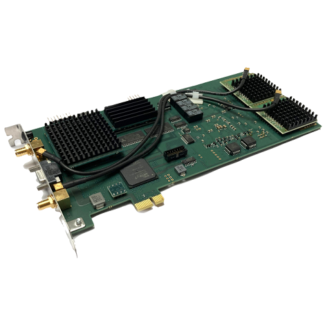
- SPC-180N, SPC-180NX, SPC-180NXX
- PCIe
- FLIM, PLIM
- Timing Precision (jitter, RMS) 2.5 ps/1.6 ps/1.1 ps
|
SPC-180N |
SPC-180NX |
SPC-180NXX |
|||
|
Photon Channel |
|
||||
|
Principle |
Constant Fraction Discriminator (CFD) |
||||
|
Discriminator Input Bandwidth |
4 GHz |
||||
|
Time Resolution (FWHM/RMS, electr.) |
6.6 ps / 2.5 ps |
< 3.5 ps / 1.6 ps |
< 3 ps / 1.1 ps |
||
|
Variance in Time of IRF max. (RMS) |
< 0.4 ps over 100 s |
||||
|
Optimum Input Voltage Range |
-30 mV to -500 mV |
||||
|
Min. Input Pulse Width |
200 ps |
||||
|
Threshold |
0 to -250 mV |
||||
|
Zero Cross Adjust |
-100 mV to 100 mV |
||||
|
Syncronisation Channel |
|
||||
|
Principle |
Constant Fraction Discriminator (CFD) |
||||
|
Discriminator Input Bandwidth |
4 GHz |
||||
|
Optimum Input Voltage Range |
-30 mV to -500 mV |
||||
|
Min. Input Pulse Width |
200 ps |
||||
|
Threshold |
0 to -250 mV |
||||
|
Frequency Range |
0 to 150 MHz |
||||
|
Frequency Divider |
1, 2, 4 |
||||
|
Zero Cross Adjust |
-100 mV to 100 mV |
||||
|
Time-to-Amplitude Converters / ADCs |
|
||||
|
Principle |
Ramp Generator / Biased Amplifier |
||||
|
TAC Range |
50 ns to 5 µs |
25 ns to 2.5 µs |
12.5 ns to 50 ns |
||
|
Biased Amplifier Gain |
1 to 15 |
||||
|
Biased Amplifier Offset (of TAC Range) |
0 % to 50 % |
||||
|
Time Range incl. Biased Amplifier |
3.3 ns to 5 µs |
1.67 ns to 2.5 µs |
0.834 ns to 50 ns |
||
|
Min. Time Channel Width |
813 fs |
407 fs |
203 fs |
||
|
ADC Principle |
50 ns Flash ADC with Error Correction |
||||
|
Diff. Nonlinerarity |
< 0.5 % RMS, typ. < 1 % peak-peak |
||||
|
Data Acquisition |
Histogram Mode |
||||
|
Method |
on-board multi-dim. histogramming process |
||||
|
Dead Time |
80 ns, independent of computer speed |
||||
|
Saturated Count Rate |
12 MHz |
||||
|
Max. Counts / Time Channel |
16 bits |
||||
|
Overflow Control |
none, stop, repeat and correct |
||||
|
Collection Time |
0.1 µs to 100,000 s |
||||
|
Diplay Interval Time |
10 ms to 100,000 s |
||||
|
Repeat Time |
0.1 µs to 100,000 s |
||||
|
Sequencing Recording |
Programmable Hardware Sequencer, unlimited recording by Memory swapping, in curve mode and scan mode |
||||
|
Syncronisation with Scanning |
Pixel, Line and Frame from Scanning Device |
||||
|
Routing |
7 bit, TTL |
||||
|
Experiment Trigger |
TTL |
||||
|
Data Acquisition |
FIFO / Parameter-Tag Mode |
||||
|
Method |
Time and wavelength tagging of individual photons and continuous writing to disk |
||||
|
Online Display |
Decay functions, FCS, Cross-FCS, PCH MCS Traces |
||||
|
FCS Calculation |
Multi-tau algorithm, online calculation and online fit |
||||
|
Number of Counts of Decay/ Waveform Recording |
unlimited |
||||
|
Dead Time |
80 ns |
||||
|
Saturated Count Rate, Peak |
12 MHz |
||||
|
Sustained Count Rate (Bus Transfer Limit) |
typ. 5 MHz |
||||
|
Max. Counts / Time Channel (Counting Depth) |
unlimited |
||||
|
Output Data Format (ADC / Macrotime / Routing) |
12 / 12 / 4 |
||||
|
FIFO Buffer Capacity (Photons) |
2 * 106 |
||||
|
Macro Timer Resolution, Internal Clock |
25 ns, 12 bit, overflows marked by MOTF entry in data stream |
||||
|
Input Macro Timer Resolution, Clock from Sync |
10 ns to 100 ns, 12 bit, overflow marked by MOTF entry in data stream |
||||
|
Input Curve Control (external Routing) |
4 bit, TTL |
||||
|
External Event Markers |
4 bit, TTL |
||||
|
Input Count Enable Control |
1 bit, TTL |
||||
|
Input Experiment Trigger |
TTL |
||||
|
Data Acquisition |
FIFO / Parameter-Tag Imaging Mode |
||||
|
Method |
Buildingup images from time- and wavelength tagged data |
||||
|
Online Display |
up to 8 Images in different time and wavelength windows |
||||
|
Synchronisation with Scanner |
via Frame Clock, Line Clock and Pixel Clock Pulses |
||||
|
Detector / Wavelength Channels |
1 to 16 |
||||
|
Image resolution (64-bit SPCM Software) |
|
||||
|
No. of Time Channels |
64 |
256 |
1024 |
4096 |
|
|
No. of Pixels, 1 Detector Channel |
4096 x 4096 |
2048 x 2048 |
1024 x 1024 |
512 x 512 |
|
|
No. of Pixels, 16 Detector Channels |
1024 x 1024 |
512 x 512 |
256 x 256 |
128 x 128 |
|
|
Operation Environment |
|
||||
|
PC System |
Windows 8 / 10, > 8 GB RAM, 64 bit operating system recommended |
||||
|
PC Interface |
PCIe |
||||
|
Power Consumption |
approx. 12 W from +12 V |
||||
|
Dimensions |
230 mm x 130 mm x 18 mm |
||||